A new paper (published online in Science) with experimental work from Zahid Hasan's group at Princeton has made a splash this week. In it, they argue that they see evidence in crystals of the compound TaAs for (quasi)particles that have the properties of so-called Weyl fermions. What does this mean?
I've written before about quasiparticles. The idea is, in a big system of interacting degrees of freedom (electrons for example), you can ask, how would we best describe the low energy excitations of that system? Often the simplest, most natural description of the excitations involves entities with well-defined quantum numbers like momentum, angular momentum, electric charge, magnetic moment, and even something analogous to mass. These low energy excitations are quasiparticles - they're "quasi" because they don't exist outside of the material medium in which they're defined, but they're "particles" because they have all these descriptive parameters that we usually think of as properties of material particles. In this situation, when we say that a quasiparticle has a certain mass, this is code for a discussion about how the energy of the excitation depends upon its momentum. For a non-relativistic, classical particle like a baseball, the kinetic energy \(E = p^{2}/2m\), where \(p\) is the magnitude of the momentum. So, if a quasiparticle has an energy roughly quadratic in its momentum, we can look at the number in front of the \(p^{2}\) and define it to be \(1/2m^{*}\), where \(m^{*}\) is an "effective mass".
In some materials under certain circumstances, you end up with quasiparticles with a kinetic energy that depends linearly on the momentum, \(E \sim p\). This is reminiscent of the situation for light in the vacuum, where \(E = p c\), with \(c\) the speed of light. A quasiparticle with this "linear dispersion" is said to act like it's "massless", in the same way that light has no mass yet still has energy and momentum. This doesn't mean that something in the material is truly massless - it just means that those quasiparticles propagate at a fixed speed (given by the constant of proportionality between energy and momentum). If the quasiparticle happens to have spin-1/2 (and therefore is a fermion), then it would be a "massless fermion". It turns out that graphene is an example of a material where, near certain energies, the quasiparticles act like this, and mathematically are well-described by a formulation dreamed up by Dirac and others - these are "massless Dirac fermions".
Wait - it gets richer. In materials with really strong spin-orbit coupling, you can have a situation where the massless, charged fermions have a spin that is really locked to the momentum of the quasiparticle. That is, you can have a situation where the quasiparticles are either right-handed (picture the particle as a bullet, spinning clockwise about an axis along its direction of motion when viewed from behind) or left-handed. If this does not happen only at particular momenta (or only at a material surface), but can happen over a more general energy and momentum range (and in the material bulk), these quasiparticles can be described in language formulated by Weyl, and are "Weyl fermions". Thanks to their special properties, the Weyl particles are also immune to some back-scattering (the kind of thing that increases electrical resistance). I'm being deliberately vague here rather than delving into the math. If you are very motivated, this paper is a good pedagogical guide.
So, what did the authors actually do? Primarily, they used a technique called angle-resolved photoemission spectroscopy (ARPES) to measure, in 3d and very precisely, the relationship between energy and momentum for the various quasiparticle excitations in really high quality crystals of TaAs. They found all the signatures expected for Weyl fermion-like quasiparticles, which is pretty cool.
Will this lead to faster computers, with charge moving 1000x faster, as claimed in various mangled versions of the press release? No. I'm not even sure where the writers got that number, unless it's some statement about the mobility of charge carriers in TaAs relative to their mobility in silicon. This system is a great example of how profound mathematical descriptions (formulated originally to deal with hypothetical "fundamental" high energy physics) can apply to emergent properties of many-body systems. It's the kind of thing that makes you wonder how fundamental are some of the properties we see in particle physics. Conceivably there could be some use of this material in some technology, but it is silly (and in my view unnecessary) to claim that it will speed up computers.
Monday, July 27, 2015
Saturday, July 25, 2015
The nanoscale: The edge of emergence
One of the most profound concepts to come out of condensed matter physics is the idea of emergent properties - nontrivial properties of a system that are not trivially deducible from the microscopic aspects and interactions of the underlying degrees of freedom, and that become even better defined as the system size grows. One example is the rigidity of solids: A single carbon atom is not rigid; a small cluster of carbon atoms has a countable number of discrete vibrational modes; but a large number of carbon atoms coupled by sp3 bonds becomes a diamond, one of the hardest, most mechanically rigid solids there is, so stiff that compressive sound travels at 12 km/s, 35 times faster than in air. Somehow, going from one atom to many, the concept of rigidity acquires meaning, and the speed of sound in diamond approaches a precise value.
I was recently rereading that book, and one chapter articulates Laughlin's basically dismissive take on nanoscience. He refers to it as a "carnival of baubles" - his view is that otherwise smart people get sucked into playing around at the nanoscale because it's diverting and involves fun, cool toys (i.e., everything looks cool under an electron microscope!), instead of spending their time and effort actually trying to think about deep, fundamental questions. Well, everyone is entitled to their opinion, but it won't surprise you that I disagree with much of that take. Working at the nanoscale allows us to examine how emergence works in specific cases, sets the ground work for the materials and devices of future technologies (two topics I touch on in my book), and allows us to develop new probes and techniques precisely for asking (some subset of) deep questions. Like being able to probe matter on ultrafast timescales, or over a huge temperature range, or in systems of unprecedented purity, pushing our control and manipulation of materials to the nano regime lets us ask new and different questions, and that's how we make progress and find surprises. This isn't an infatuation with baubles (though everything does look cool under an electron microscope).
Friday, July 17, 2015
A grand challenge for nano: Solar energy harvesting near the thermodynamic limit
As I'd mentioned earlier in the week, the US Office of Science and Technology Policy had issued a call for "Grand Challenges" for nanotechnology for the next decade, with a deadline of July 16, including guidelines about specific points that a response should address. Here is my shot:
Affordable solar
energy collection/conversion that approaches the thermodynamic efficiency limit
based on the temperature of the sun (efficiency approaching 85%).
Physics, specifically the second law of thermodynamics, places very strict limits on how much useful energy we can extract from physical systems. For example, if you have a big rock at temperature \(T_{\mathrm{hot}}\), and another otherwise identical big rock at temperature \(T_{\mathrm{cold}}\), you could let these two rocks just exchange energy, and they would eventually equilibrate to a temperature \(T_{0} = (T_{\mathrm{hot}}+T_{\mathrm{cold}})/2\), but we would not have gotten any useful energy out of the system. From the standpoint of extracting useful energy, that process (just thermal conduction + equilibration) would have an efficiency of zero. Instead, you could imagine running a heat engine: You might warm gas in a cylinder using the hot rock, so that its pressure goes up and pushes a piston to turn a crank that you care about, and then cool the piston back to its initial condition (so that you can run this as a cycle) by letting the gas dump energy to the cold rock. Carnot showed that the best you can do in terms of efficiency here is \( (1 - T_{\mathrm{cold}}/T_{\mathrm{hot}})\). On a fundamental level, this is what limits the efficiency of car engines, gas turbines in power plants, etc. If the "cold" side of your system is near room temperature (300 Kelvin), then the maximum efficiency permitted by physics is limited by how hot you can make the "hot" side.
So, what about solar power? The photosphere of the sun is pretty hot - around 5000 K. We can get energy from the sun in the form of the photons it radiates. Using 300 K for \(T_{\mathrm{cold}}\), that implies that the theoretical maximum efficiency for solar energy collection is over 90%. How are we doing? Rather badly. The most efficient solar panels you can buy have efficiencies around 35%, and typical ones are more like 18%. That means we are "throwing away" 60% - 80% of the energy that should be available for use. Why is that? This article (here is a non-paywall pdf) by Albert Polman and Harry Atwater has a very good discussion of the issues. In brief: There are many processes in conventional photovoltaics where energy is either not captured or is "lost" to heat and entropy generation. However, manipulating materials down to the nm level offers possible avenues for avoiding these issues - controlling optical properties to enhance absorption; controlling the available paths for the energy (and charge carriers) so that energy is funneled where it can be harnessed. On the scale of "grand challenges", this has a few virtues: It's quantitative without being fantastical; there are actually ideas about how to proceed; it's a topical, important social and economic issue; and even intermediate progress would still be of great potential importance.
Thursday, July 16, 2015
Active learning vs. lecturing: the annual hectoring
The new issue of Nature contains this article, discussing the active learning approach to teaching. Actually, "discussing" is too neutral. The title of the article and the subheadline flatly state that lecture-based pedagogy is "wrong". The article includes this quote about active learning: " 'At this point it is unethical to teach any other way' ", and presents that quote as a bold-face callout.
The article says "Researchers often feel that a teacher's job is simply to communicate content: the factual knowledge covered in the course." This is an assertion, and based on my experience, one that is incorrect. If basic communication of facts is the job of teachers, we should just quit now, since books and more recently google have made us obsolete. The whole point of in-person instruction is more than conveying a list of facts - in the case of physics, it's a matter of teaching people how to think about the world, how to think critically and translate concepts and ideas into the language of mathematics for the purposes of gaining predictive understanding and an appreciation for the beautiful way the universe works.
The article also implies that faculty are reluctant to migrate to active learning because it would require that we work harder (i.e., greater prep time, and therefore less time for research) to achieve its benefits. I do think it was good for the author to raise the issue of incentives and rewards at the end: If universities want to claim that they value teaching, they actually need to reward pedagogy.
By trying to cast active learning vs lecture-based pedagogy as a one-size-fits-all, good vs bad, modernists vs sticks-in-the-mud faceoff, the author does a disservice to the genuinely subtle questions at play here. Yes, it looks like well-done active learning does enable large segments of the target audience (typically in intro courses) to retain concepts better. Not all active learning approaches are implemented well, however; some lecturers can be outstanding, and the ones that engage the class in discussion and back-and-forth are blurring the line into active learning anyway; active learning definitely is a compromise in that the investment of personnel and time to achieve the benefits does mean leaving out some content; and different people learn best from different methods! The author raises these issues, but the main thesis of the article is clear.
I want to raise a question that you will find in many physics departments around the US: Who is the target audience in our classes, particularly beyond the large freshmen service teaching courses? In a big intro class with 350 future engineers, or 400 pre-meds, maybe sacrificing some content for the sake of engaging a larger fraction of the students to better internalize and retain physical concepts is a good idea. If we do this, however, in a way that bores or fails to challenge the top students, or leaves gaps in terms of content, is that a net good?
My point: Pedagogy is complicated, and in the sciences and engineering we are trying to do several competing tasks in parallel. Oversimplifying to the level that "active learning = unalloyed good all the time; traditional lecture = unethical, abusive method clung to by lazy, hidebound, research-driven-teaching-averse faculty" is not helpful.
Sunday, July 12, 2015
Nano "Grand Challenges" for the next decade
Last month the White House Office of Science and Technology Policy issued a call for suggestions for "nanotechnology-inspired grand challenges". The term "grand challenge" is popular, both within the federal agencies and among science/technology coordinating and policy-making groups. When done well, a list of grand challenges can cleanly, clearly articulate big, overarching goals that a community has identified as aspirational milestones toward which to strive. When done poorly, a list of grand challenges can read like naive fantasy, with the added issue that pointing this out can lead to being labeled "negative" or "lacking in vision". To make up a poor example: "In the next ten years we should develop a computing device smaller than a grain of rice, yet more powerful than an IBM Blue Gene supercomputer, able to operate based on power acquired from the ambient environment, and costing less than $5 to manufacture." Yeah, not too realistic.
It's worth thinking hard about these, though, and trying to contribute good ones. The deadline for this call is this coming Thursday, so get yours in while you can. I put one in that I will discuss later in the week.
It's worth thinking hard about these, though, and trying to contribute good ones. The deadline for this call is this coming Thursday, so get yours in while you can. I put one in that I will discuss later in the week.
Friday, July 10, 2015
What do IBM's 7 nm transistors mean?
Two days ago IBM and their consortium partners made a big splash by announcing that they had successfully manufactured prototype chips on the wafer scale (not just individual devices) with features compatible with the 7 nm "node". What does that mean? It's being reported that the transistors themselves are "7 nm wide". Is that correct?

The term "node" is used by the semiconductor industry to characterize major targets in their manufacturing roadmap. See here for more information that you could ever possibly want about this. The phrase "xx nm node" means that the smallest spacing between repeated features on a chip along one direction is xx nm. It does not actually mean that transistors are now xx nm by xx nm. Right now, the absolute state of the art on the market from Intel are chips at the 14 nm node. A cross-section of those taken by transmission electron microscope is shown to the right (image from TechInsights), and Intel has a nice video explaining the scheme here. The transistors involve fin-shaped pieces of silicon - each fin is about 14 nm wide, 60-70 nm tall, and a hundred or more nm long. One transistor unit in this design contains two fins each about 40 nm apart, as you can see in the image. The gate electrode that cuts across the fins is actually about 40-50 nm in width. I know this is tough to visualize - here is a 3-fin version, annotated from a still from Intel's video. In these devices current flows along the long direction of the fin, and the gate can either let the current pass or not, depending on the voltage applied - that's how these things function as switches.

So: The 7 nm node IBM chip is very impressive. However, don't buy into the press release wholesale just yet - there is a lot of ground to cover before it becomes clear that these chips are really "manufacturable" in the sense commonly used by the semiconductor industry.
I'll touch on two points here. First, yield. The standard architecture of high performance logic chips these days assumes that all the transistors work, and we are talking about chips that would contain several billion transistors each. In terms of manufacturing and reliability, integrated semiconductor devices are freaking amazing and put mechanical devices to shame - billions of components connected in a complicated way, and barring disaster these things can all work for many years at a time without failure. To be "manufacturable", chip makers need to have the yield of good chips (chips where all the components actually work) be high enough to cover the manufacturing costs at a reasonable price point. That typically means yield rates over at least 30%. Back in the '90s Intel was giving its employees keychains made from dead Pentium processors. It's not at all clear that IBM can really make these chips with good yields. Note that Intel recently delayed manufacturing of 10 nm node chips because of problems.
Second, patterning technology. All chips in recent years (including Intel's 14 nm and even their prototype 10 nm node products) are patterned using photolithography, based on a light source with a wavelength of 193 nm (!). Manufacturers have relied on several bits of extreme cleverness to pattern features down to 1/20 of the free-space wavelength of the light, including immersion lithography, optical phase control, exotic photochemistry, and multiple patterning. However, those can only carry you so far. IBM and their partners have decided that now is finally the time to switch to a new light source, 13.5 nm wavelength, the so-called extreme ultraviolet. This has been in the planning stages for years, with prototype EUV 300 mm wafer systems at Albany Nanofab and IMEC for about a decade. However, changing to new wavelengths and therefore new processing chemistry and procedures is fraught with challenges. I'm sure that IBM will get there, as will their competitors eventually, but it wouldn't shock me if we don't see actual manufacturing of 7 nm node chips for four or five more years at least.
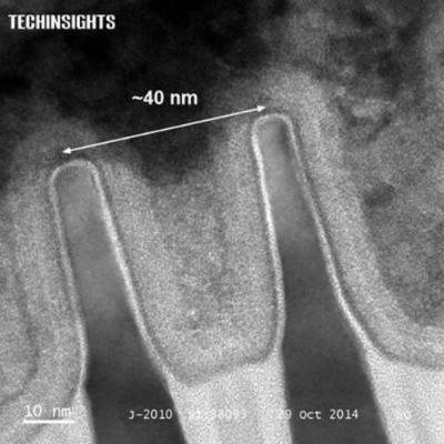
Monday, July 06, 2015
Ten years of blogging about CMP/nano
A couple of weeks ago this blog passed through its tenth anniversary (!). That makes me about 70 in blog-years. At the time, science blogging was going through a rapid expansion, and since then there has been a major die-off (we still miss you, Incoherent Ponderer) - people decide that they aren't reaching their desired audience, or don't have the time, or have run out of things to say, etc.
A lot has happened in nanoscience and condensed matter physics in the last decade: the rise of graphene (a late post on this), the recognition of topological insulators, the discovery of the iron pnictide superconductors, observations related to Majorana fermions, to name a few. It's been fun to watch and discuss. I've written quite a bit (but not so much recently) on physics as as undergrad and cultural attitudes, choosing a grad school, choosing/finding a postdoc position, giving talks in general, trying to get a faculty job, and other career-oriented topics, as well as science policy. Over time, I've leaned more toward trying to explain CMP and nano concepts in more accessible ways, and at least identifying why this can sometimes be more difficult in our discipline than in high energy physics.
Anyway, it's been a lot of fun, and I'm not going anywhere, thanks in large part to knowing that you are actually continuing to read this. Thanks for your support. If there are particular topics you'd like to see, please comment as always.
Sunday, July 05, 2015
Can we use machine learning to solve really hard physics problems?
One of the most important achievements in 20th century physics and chemistry is density functional theory (DFT). In 1964, Walter Kohn and Pierre Hohenberg proved a rather amazing result: If you want to know the ground state electronic properties of any condensed quantum electronic system (e.g., a solid, or a molecule), you can get all of that information (even in a complicated, interacting, many-body system!) just from knowing the ground state electronic density everywhere, \(n(\mathbf{r})\). That is, any property you might care about (e.g., the ground state energy) can be computed from \(n(\mathbf{r})\) as a functional \(F[n(\mathbf{r})]\). (A functional is a function of a function - in this case \(F\) depends in detail on the value of \(n\) everywhere.) The Hohenberg-Kohn paper is the most-cited physics paper of all time, suggesting its importance. So, truly figuring out the electronic structure of molecules and materials just becomes a matter of figuring out an extremely good approximation to \(n(\mathbf{r})\).
Moreover, Kohn and Lu Sham then went further, and found a practical calculational approach that lets you work with an effective system of equations to try to find \(n(\mathbf{r})\) and the ground state energy. In this formulation, they write the total energy functional \(E[n(\mathbf{r}]\) as a sum of three pieces: a kinetic energy term that may be written as a comparatively simple expression; a potential energy term that is easy to write and simply interpreted as the Coulomb repulsion; and the third bit, the "exchange-correlation functional", \(E_{\mathrm{xc}}[n(\mathbf{r})]\), which no one knows how to write down analytically.
You might think that not knowing how to write down an exact expression for \(E_{\mathrm{xc}}[n(\mathbf{r})]\) would be a huge issue. However, people have come up with many different approximation methods, and DFT has been hugely useful in understanding the electronic properties of solids and molecules.
In recent years, though, some people have been wondering if it's possible to use "machine learning" - essentially having a computer derive an extremely good look-up table or interpolation - to approach an exact description of \(E_{\mathrm{xc}}[n(\mathbf{r})]\). This is not a crazy idea at all, based on engineering history and dimensional analysis. For example, actually writing down an analytical expression for the pressure drop of water flowing through a rough pipe is not generally possible. However, dimensional analysis tells us that the pressure drop depends on just a couple of dimensionless ratios, and a zillion experiments can be run to map out a look-up table for what that un-writable multivariable function looks like. Perhaps with computers that are becoming incredibly good at identifying patterns and underlying trends, we can do something similar with \(E_{\mathrm{xc}}[n(\mathbf{r})]\). One of the main groups pursuing this kind of idea is that of Keiran Burke, and last week a preprint appeared on the arxiv from others arguing that machine learning can be useful in another many-body approach, dynamical mean field theory. Who knows: Maybe someday the same types of algorithms that guess songs for you on Pandora and book suggestions on Amazon will pave the way for real progress in "materials by design"!
Subscribe to:
Posts (Atom)